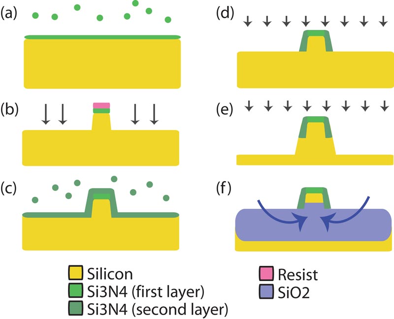
| Process flow: (a) bulk silicon wafer and silicon nitride deposition; (b) ICP etch; (c) second deposition of silicon nitride; (d) ICP cap etch; (e) extended etch for quicker oxidation; (f) extended wet oxidation for waveguide underlayer flattening. (Image credit: Nicolas Sherwood-Droz) |
| © 2024 SPIE Europe |
|