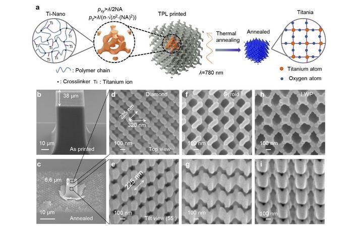
| Figure 1. (a) Schematic of the fabrication process. (b) Scanning electron microscope (SEM) image of an as-printed diamond PhC. (c) Tile view SEM image of the annealed diamond PhC. (d-i) High-magnification SEM images of the top and tilt view of the annealed diamond (d-e), gyroid (f-g) and I-WP (h,i) PhCs, respectively. Credit: SUTD. |
| © 2024 SPIE Europe |
|