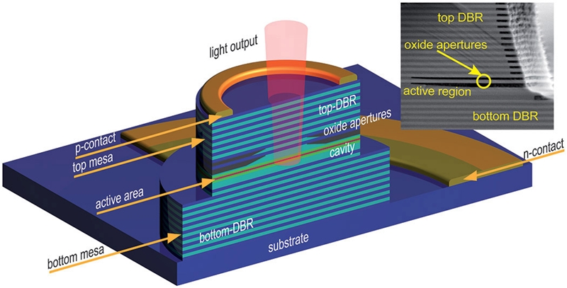
| A typical GaAs VCSEL structure. The layers of compound semiconductor material that make up the device's active elements are deposited using specialist techniques. Anadigics has developed a manufacturing process on a 6-inch wafer platform that II-VI wants to ramp for emerging applications in consumer electronics as well as the existing data center market. Image courtesy of SPIE/TU Berlin. |
| © 2024 SPIE Europe |
|